Wafer Inspection at Advanced Nodes: Detecting Patterned Wafer Defects with Dark-Field and UV Imaging
The Growing Challenge of Patterned Wafer Inspection
Semiconductor wafer inspection has become a defining factor for yield, reliability, and time-to-market. As devices shrink, patterned wafer inspection becomes more difficult due to dense layouts and complex structures that reduce visual contrast. This allows critical defects to blend into intended features.
Dark‑field inspection is an optical inspection technique used in semiconductor manufacturing that detects defects by capturing scattered light rather than reflected light.
Traditional bright‑field approaches often struggle to reveal certain defect types, making alternative inspection modes essential.
Seeing What Bright‑Field Misses
Dark-field inspection excels at detecting surface-related defects on patterned wafers. Pattern edge defects, micro‑bridges, and hairline scratches generate minimal reflected‑light contrast but scatter light strongly. In dark‑field mode, these disruptions stand out clearly, enabling earlier semiconductor defect detection of issues that may cause shorts or opens.
This approach is also highly effective for detecting very small particle contamination. At advanced nodes, even particles smaller than the pattern pitch can impact yield. While bright‑field inspection may have difficulty distinguishing particles from the patterned background, dark‑field imaging improves visibility by emphasizing scattered light.
Improving Defect‑to‑Pattern Contrast in Wafer Inspection
Beyond sensitivity, fabs must manage nuisance signals created by dense patterned structures. Dark‑field inspection helps defects stand out by amplifying scattered light from irregular features such as particles, scratches, or edge disruptions.
When combined with optimized inspection algorithms, this improved contrast helps distinguish true semiconductor defect detection signals from normal pattern variations. The result is reduced unnecessary review effort and improved inspection efficiency.
Extending Dark‑Field Inspection with Ultraviolet Imaging
As device dimensions continue to shrink, inspection performance increasingly depends on wavelength selection. When feature sizes approach the limits of visible light, inspection sensitivity can become constrained. Ultraviolet imaging enhances dark-field inspection effectiveness by using shorter wavelengths that interact strongly with nanoscale edges and particles.
In patterned wafer inspection, UV dark‑field imaging provides:
- Enhanced scattering from fine edge defects
- Improved detection of sub‑pitch particle contamination
- Higher defect‑to‑pattern contrast in dense layouts
- By optimizing dark‑field inspection for advanced‑node physics, UV imaging enables earlier defect detection and stronger yield protection.
UV Camera Solutions for Advanced Wafer Inspection
Exosens offers ultraviolet camera solutions (i2Nocturn and iNocturn series) designed for dark-field wafer inspection applications. These cameras are engineered to deliver high sensitivity, low noise, and stable performance at UV wavelengths, supporting consistent defect detection on advanced patterned wafers.
Key benefits include:
- Optimized UV quantum efficiency for enhanced scattering detection
- High sensitivity for subtle defect signals
- Low‑noise imaging for improved defect‑to‑pattern discrimination
- Compatibility with dark‑field inspection architectures
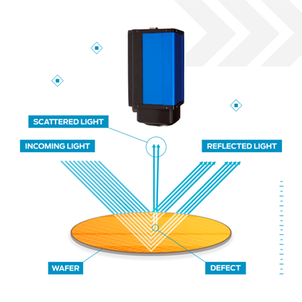
Figure 1. Schematic of dark‑field illumination showing scattered light collected from surface defects with i2Nocturn camera.
Whether used in process development, inline inspection, or failure analysis, UV imaging helps extend wafer inspection capabilities beyond visible‑light constraints.

Seeing What Matters at Nanoscale Dimensions
Dark-field inspection plays an important role in modern patterned wafer inspection by helping reveal edge defects, small particles, and low-contrast disruptions in dense layouts. As device scaling continues, ultraviolet imaging provides a natural extension, enhancing dark-field sensitivity without changing the underlying inspection approach.
By combining dark-field architectures with purpose-built UV cameras, fabs gain the visibility required to detect critical defects before they impact yield, performance, or time to market.
Related content

Naples.

Jun 08th 2026
Seeing Beyond the Visible Battlefield
Imaging Solutions for Decisive Defense Advantage

May 26th 2026
Europe’s Infrared Defense Sovereignty
Exosens contributes to Europe’s stratégic defense sovereignty in infrared sensing through SPIRIT initiative

May 25th 2026
Exosens aboard ESA’s SMILE Mission
Exosens Enables Breakthrough X-Ray Imaging onboard ESA/CAS SMILE Mission

Paris.
FROM Jun 02nd 2026 TO Jun 05th 2026
Société Française de Thermique 2026
Join Exosens at the 34th Annual Congress of the Société Française de Thermique 2026

May 20th 2026
Exosens Doubles Cooled IR Camera Production
Exosens Doubles Production Capacity for Cooled Infrared Cameras to Meet Accelerating Demand in Long-Range Counter-drone systems
